How Semiconductors are Made
Understanding the remarkable process of turning sand into thinking machines.
Table of contents
- Introduction: Teaching Sand to Think
- From Sand to Silicon
- The Photolithography Process
- Transistor Formation
- Integration and Packaging
- Modern CPU Architecture
- Manufacturing Challenges
- Hands-On Activity: Visualizing Scale
- The Future of Semiconductor Manufacturing
- Next Steps
- Additional Resources
Introduction: Teaching Sand to Think
Semiconductors are the foundation of all modern computing devices. These remarkable components, primarily made from silicon, enable the billions of transistors that power our digital world. The journey from raw sand to functioning computer chips is one of the most sophisticated manufacturing processes humans have ever developed.
From Sand to Silicon
Silicon Extraction
The process begins with silicon dioxide (SiO₂), commonly found in sand. However, not just any sand will do:
- Raw Material Selection: High-purity quartz sand is selected
- Reduction Process: The sand is heated with carbon to remove oxygen
- Initial Purification: Resulting in metallurgical-grade silicon (98-99% pure)
- Chemical Purification: Converted to liquid compounds, then distilled
- Final Purification: Resulting in electronic-grade silicon (99.9999999% pure)
Creating Silicon Ingots
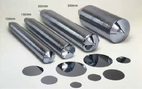
Once purified, the silicon is formed into large, cylindrical ingots:
- Seed Crystal: A small perfect crystal provides the structure
- Czochralski Process: The seed is dipped into molten silicon and slowly pulled upward
- Crystal Growth: As the seed rotates and rises, silicon solidifies in a perfect crystal structure
- Ingot Formation: The result is a large cylindrical ingot of single-crystal silicon
Wafer Slicing and Preparation
The ingots are then sliced into thin wafers:
- Diamond Sawing: Ingots are cut into thin wafers (less than 1mm thick)
- Edge Rounding: Wafer edges are rounded to prevent chipping
- Polishing: Wafers are polished to achieve an ultra-flat, mirror-like surface
- Cleaning: Multiple cleaning steps remove any particles or contaminants
The Photolithography Process
Photolithography is the key process that creates the intricate patterns of transistors on silicon:
Photoresist Application
- Wafer Preparation: The wafer is cleaned and heated
- Photoresist Coating: A light-sensitive chemical is applied evenly
- Soft Baking: The photoresist is baked to improve adhesion
Mask Alignment and Exposure
- Photomask Creation: A “stencil” containing the circuit pattern is created
- Alignment: The mask is precisely aligned with the wafer
- Exposure: Ultraviolet light shines through the mask onto the photoresist
- Pattern Transfer: The UV light changes the chemical properties of exposed photoresist
Etching and Doping
- Development: The exposed photoresist is removed, revealing the pattern
- Etching: Chemicals remove silicon in the exposed areas
- Photoresist Removal: Remaining photoresist is stripped away
- Doping: Adding impurities (like boron or phosphorus) to change electrical properties
Transistor Formation
Modern chips contain billions of transistors, each created through multiple photolithography cycles:
Building Layers
- Gate Oxide: A thin insulating layer is grown
- Polysilicon Deposition: Gate material is deposited
- Source/Drain Formation: Areas for current flow are created
- Metal Interconnects: Aluminum or copper connections between transistors
- Insulating Layers: Silicon dioxide layers separate the metal layers
Creating Connections
- Via Formation: Holes are etched through insulating layers
- Metal Filling: Vias are filled with metal to connect different layers
- Planarization: Surfaces are flattened for the next layer
Integration and Packaging
Once the wafer processing is complete:
Die Cutting
- Wafer Testing: Each die (chip) is tested while still on the wafer
- Wafer Mapping: Defective dies are mapped and marked
- Dicing: The wafer is cut into individual dies
Testing
- Initial Testing: Basic functionality verification
- Burn-in Testing: Stress testing under elevated temperatures
- Speed Grading: Chips are sorted by performance capabilities
Packaging and Final Assembly
- Die Attachment: The silicon die is attached to a substrate
- Wire Bonding: Tiny wires connect the die to package pins
- Encapsulation: Protective material covers the die and connections
- Final Testing: Complete functional testing of the packaged chip
Modern CPU Architecture
Modern CPUs have evolved far beyond simple processing units:
Advanced Architectures
- Multi-core Design: Multiple processing cores on a single die
- Hyperthreading: Virtual cores that improve multitasking
- Cache Hierarchy: Multiple levels of increasingly larger cache
- Specialized Units: Dedicated circuits for graphics, AI, encryption
- Chiplet Design: Multiple smaller dies connected together
Transistor Evolution
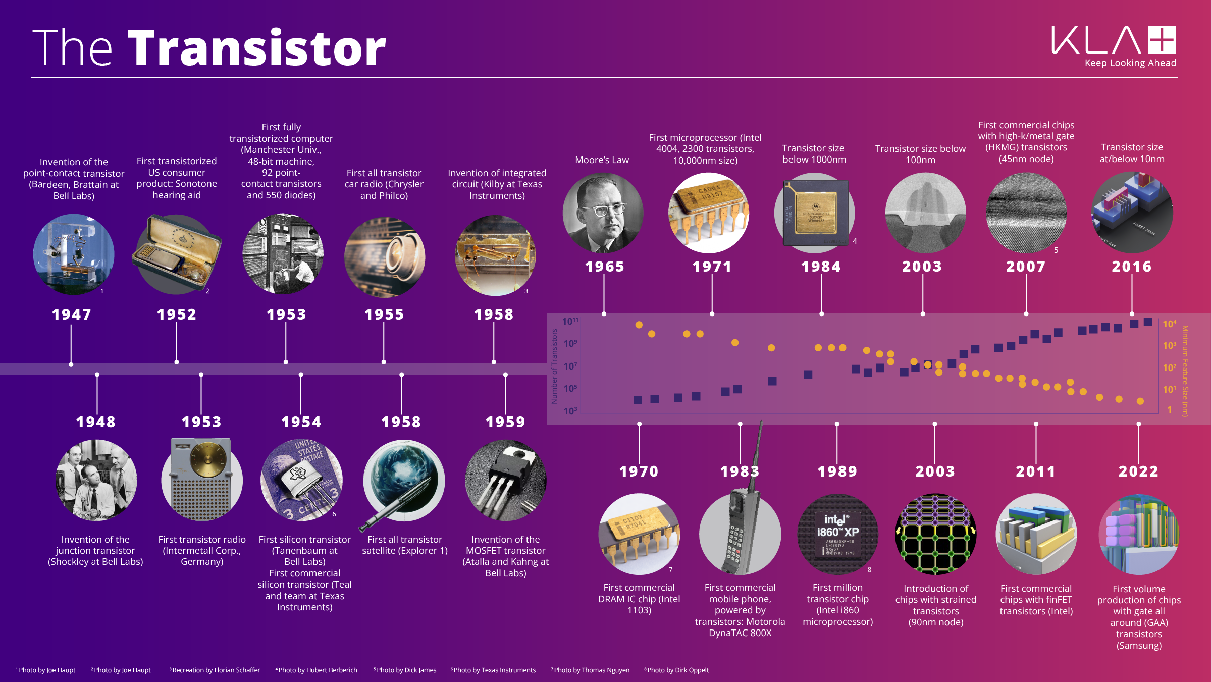
The evolution of transistors over the past 75 years represents one of the most remarkable technological achievements in human history:
- 1947: The first transistor at Bell Labs - large enough to hold in your hand
- 1960s: Early integrated circuits with dozens of transistors
- 1970s: Thousands of transistors on early microprocessors
- 1980s-1990s: Millions of transistors as manufacturing improved
- 2000s: Billions of transistors as nanometer-scale processes matured
- Today: Trillions of transistors in advanced systems with transistors just a few nanometers in size
This exponential improvement has enabled the computing revolution, from room-sized computers to smartphones billions of times more powerful that fit in your pocket.
Manufacturing Challenges
Nanometer-Scale Processes
- Quantum Effects: At tiny scales, quantum physics affects transistor behavior
- Heat Dissipation: Smaller transistors generate more heat per area
- Lithography Limits: Pushing the boundaries of physics to create smaller features
- Interconnect Delays: Signal delays between transistors become significant
Clean Room Requirements
- Class 1 Clean Rooms: Less than 1 particle per cubic foot
- Vibration Control: Buildings designed to minimize vibrations
- Temperature Control: Maintained within ±0.1°C
- Special Clothing: “Bunny suits” prevent contamination
Yield Management
- Defect Detection: Advanced imaging to find nanoscale defects
- Redundancy: Building spare components into designs
- Binning: Sorting chips by quality and performance
- Constant Improvement: Statistical process control to improve yields
Hands-On Activity: Visualizing Scale
To appreciate the scale of modern semiconductor manufacturing:
# Relative scale comparison:
Human hair width: ~100,000 nm
Bacteria: ~1,000 nm
Virus: ~100 nm
Modern transistor: ~5-10 nm
Silicon atom: ~0.2 nm
The Future of Semiconductor Manufacturing
Emerging Technologies
- 3D Stacking: Vertical integration of transistors
- New Materials: Beyond silicon (graphene, carbon nanotubes)
- Quantum Computing: Using quantum properties for computation
- Neuromorphic Computing: Brain-inspired architectures
Economic and Strategic Importance
- Global Supply Chains: Semiconductor manufacturing spans continents
- National Security: Considered critical infrastructure by many countries
- Massive Investment: New fabrication plants cost $10-20 billion
- Research Intensity: Constant innovation required to advance
Next Steps
Continue to explore computer hardware concepts:
- Review CPU Basics for more on processor architecture
- Learn about RAM Basics to understand memory technology
- Explore Computer Hardware Overview for the broader context