CPU Basics: The Brain of Your Computer
Understanding how the Central Processing Unit works and why it matters.
Table of contents
- What is a CPU?
- CPU Components
- The CPU Instruction Cycle
- CPU Performance Factors
- CPU Optimization Techniques
- CPU Manufacturers and Families
- CPU Cooling
- Overclocking
- Hands-On: Monitoring Your CPU
- Future of CPU Technology
- Next Steps
- Additional Resources
What is a CPU?
The Building Blocks: Transistors
At the heart of every CPU are billions of tiny electronic switches called transistors:
- Transistors are semiconductor devices that can amplify or switch electronic signals
- Modern CPUs contain billions of transistors (Apple’s M3 Ultra has over 134 billion transistors)
- Transistors are arranged into logic gates that perform basic operations (AND, OR, NOT, etc.)
- These logic gates are combined to create more complex circuits like adders, multiplexers, and registers
- The size of transistors is measured in nanometers (nm), with current cutting-edge processes at 3-5nm
The Central Processing Unit (CPU) is often called the “brain” of the computer. It’s responsible for executing instructions, performing calculations, and coordinating the activities of all other components in the computer system.

Every action you take on a computer—from clicking a button to running complex software—involves the CPU processing instructions. The CPU’s performance largely determines how quickly your computer can complete tasks.
CPU Components
A modern CPU contains several key components that work together:
Arithmetic Logic Unit (ALU)
The ALU performs all arithmetic and logical operations:
- Arithmetic operations: Addition, subtraction, multiplication, division
- Logical operations: AND, OR, NOT, XOR, comparisons (equal to, greater than, etc.)
The ALU takes input from registers, performs operations, and stores results back in registers.
Registers
Registers are small, high-speed storage locations within the CPU:
- Data registers: Store operands and results of ALU operations (A and B registers)
- Accumulator: Stores the result of arithmetic and logical operations
- Instruction register: Holds the current instruction being executed
- Instruction pointer: Contains the address of the next instruction to fetch
- Status register: Contains flags indicating the status of operations (zero, carry, overflow, etc.)
Registers are the fastest form of data storage in a computer, but they are very limited in number and size.
Control Unit
The control unit coordinates the activities of all CPU components:
- Fetches instructions from memory
- Decodes instructions to determine required operations
- Executes instructions by sending signals to the appropriate components
- Manages the timing of operations using the CPU clock
Cache Memory
Cache memory is high-speed memory located on or close to the CPU:
- L1 cache: Smallest but fastest cache, typically split into instruction (L1i) and data (L1d) caches
- L2 cache: Larger but slightly slower than L1
- L3 cache: Largest but slowest of the CPU caches, often shared among all cores
Cache memory stores frequently accessed data and instructions to reduce the time spent waiting for data from main memory (RAM).
Memory Management Unit (MMU)
The MMU handles all memory operations:
- Translates virtual memory addresses to physical addresses
- Manages memory protection and access rights
- Facilitates paging and swapping between RAM and disk storage
The CPU Instruction Cycle
The CPU operates by repeatedly executing a sequence of operations known as the instruction cycle or fetch-decode-execute cycle:

1. Fetch
The CPU retrieves the next instruction from memory:
- The address in the instruction pointer is sent to memory
- The instruction at that address is loaded into the instruction register
- The instruction pointer is incremented to point to the next instruction
2. Decode
The control unit interprets the instruction:
- The instruction is broken down into components
- The operation to be performed is identified
- The operands (data to be operated on) are located
3. Execute
The CPU performs the operation:
- The ALU carries out arithmetic or logical operations
- Data is transferred between registers, memory, or I/O devices
- The program counter may be modified for jump or branch instructions
4. Store
The results are written back:
- Results are stored in registers or memory
- Status flags are updated based on the operation’s outcome
This cycle repeats millions or billions of times per second, driven by the CPU clock.
CPU Performance Factors
Several factors affect CPU performance:
Clock Speed
Clock speed, measured in gigahertz (GHz), indicates how many cycles the CPU can perform per second:
- A 3.2 GHz processor can perform 3.2 billion cycles per second
- Higher clock speeds generally mean faster processing
- However, comparing clock speeds is only meaningful between CPUs of the same architecture
Number of Cores
Modern CPUs contain multiple processing cores:
- Each core is essentially a separate processor capable of executing instructions independently
- More cores allow for better multitasking and parallel processing
- Common configurations include dual-core, quad-core, hexa-core, octa-core, and more
- Software must be written to take advantage of multiple cores (multithreaded applications)
Performance (P) and Efficiency (E) Cores
Modern CPU designs, particularly from Intel and ARM, now implement a hybrid architecture with two types of cores:
- Performance (P) cores: Larger, more powerful cores designed for maximum performance
- Handle demanding tasks like gaming, video editing, and complex calculations
- Higher clock speeds, more cache, and advanced features like hyperthreading
- Consume more power and generate more heat
- Efficiency (E) cores: Smaller, more power-efficient cores for background tasks
- Handle lightweight tasks like web browsing, email, and system processes
- Lower clock speeds and simpler designs that use less power
- Allow the system to save energy when maximum performance isn’t needed
This hybrid approach, sometimes called “big.LITTLE” (ARM) or “Performance-Hybrid” (Intel), allows for better power efficiency without sacrificing peak performance. The operating system’s scheduler determines which tasks run on which type of core.
Cache Size
The amount of cache memory affects how often the CPU needs to access slower main memory:
- Larger caches generally improve performance
- L1 cache sizes typically range from 64 KB to 512 KB
- L2 cache sizes typically range from 256 KB to 2 MB per core
- L3 cache sizes typically range from 4 MB to 64 MB (shared among cores)
Instruction Set Architecture (ISA)
The instruction set defines the operations a CPU can perform:
- Common ISAs include x86, x86-64 (AMD64), ARM, and RISC-V
- CISC (Complex Instruction Set Computer) architectures like x86 have many specialized instructions
- RISC (Reduced Instruction Set Computer) architectures like ARM focus on simpler, more efficient instructions
Microarchitecture
The internal design of the CPU affects how efficiently it executes instructions:
- Pipeline depth: More pipeline stages can allow higher clock speeds but may increase latency
- Branch prediction: Better prediction reduces pipeline stalls
- Out-of-order execution: Allows instructions to execute when their operands are ready, not necessarily in program order
- Speculative execution: Executes instructions before knowing if they’re needed, improving performance when predictions are correct
CPU Optimization Techniques
Modern CPUs employ several techniques to improve performance:
Pipelining
Pipelining breaks instruction execution into stages that can operate simultaneously:
- While one instruction is being executed, the next can be decoded, and a third can be fetched
- Increases throughput (instructions per second) without requiring faster components
- Most modern CPUs have pipelines with 10-20 stages

Hyperthreading
Hyperthreading (Intel) or Simultaneous Multithreading (AMD) allows a single physical core to act as two logical cores:
- Duplicates certain portions of the processor but not the main execution resources
- When one thread is waiting (e.g., for data from memory), the other can execute
- Can improve performance by 15-30% in multithreaded applications
Branch Prediction
Branch prediction attempts to guess which path a program will take before the condition is evaluated:
- Modern CPUs can predict with 90%+ accuracy for many workloads
- Correct predictions allow the pipeline to continue without stalls
- Incorrect predictions require flushing the pipeline and restarting, causing performance penalties
Superscalar Execution
Superscalar processors can execute multiple instructions per clock cycle:
- Multiple execution units operate in parallel
- Instructions are analyzed for dependencies and executed when possible
- Can achieve more than one instruction per cycle (IPC > 1)
CPU Manufacturers and Families
The CPU market is dominated by a few major manufacturers:
Intel
Intel is one of the oldest and largest CPU manufacturers:
- Core series: Mainstream processors (i3, i5, i7, i9)
- Xeon: Server and workstation processors
- Celeron and Pentium: Budget processors
- Atom: Low-power processors for mobile devices
AMD
AMD (Advanced Micro Devices) is Intel’s primary competitor:
- Ryzen: Mainstream processors (Ryzen 3, 5, 7, 9)
- EPYC: Server processors
- Athlon: Budget processors
- Threadripper: High-end desktop processors
ARM
ARM Holdings designs CPU architectures that are licensed to manufacturers:
- Used in most smartphones and tablets
- Apple’s M1/M2/M3 chips are based on ARM architecture
- Known for energy efficiency
- Increasingly used in laptops and even servers
Apple Silicon
Apple’s custom ARM-based processors represent a significant shift in CPU design philosophy:
- Unified Memory Architecture (UMA): Unlike traditional systems where CPU and GPU have separate memory pools, Apple Silicon uses a shared memory architecture
- CPU, GPU, Neural Engine, and other components all access the same memory pool
- Eliminates the need to copy data between different memory spaces
- Dramatically reduces latency and increases bandwidth
- Allows for more efficient use of available memory
- System-on-Chip (SoC) Design: Integrates CPU, GPU, Neural Engine, memory, and various controllers on a single chip
- Reduces physical distance between components
- Lowers power consumption
- Improves overall system efficiency
- High-Bandwidth Memory: Apple Silicon incorporates high-speed memory directly into the SoC package
- Memory is physically closer to the processing units than in traditional designs
- Uses wider memory buses (up to 512-bit in M3 Ultra) for massive bandwidth
- Provides up to 192GB of unified memory in high-end configurations
- Memory bandwidth can exceed 800GB/s in top models
Console Processors and Unified Memory
Modern gaming consoles like PlayStation 5 and Xbox Series X/S use a similar unified memory approach:
- Both use custom AMD SoCs with integrated CPU and GPU
- Both implement a unified memory architecture where the CPU and GPU share a single, high-speed memory pool
- This allows for extremely fast data transfer between CPU and GPU processing
- Eliminates traditional bottlenecks in gaming performance
- Enables developers to use memory more flexibly and efficiently
The unified memory approach in both Apple Silicon and modern consoles represents a significant architectural advantage over traditional PC designs, where separate CPU and GPU memory pools create data transfer bottlenecks.
Other Manufacturers
- IBM: Power architecture for servers and mainframes
- RISC-V: An open-source ISA with growing adoption
- Qualcomm: Snapdragon processors for mobile devices (ARM-based)
- Samsung: Exynos processors for mobile devices (ARM-based)
CPU Cooling
CPUs generate significant heat during operation and require cooling to prevent damage:
Air Cooling
- Heat sink: Metal structure that draws heat away from the CPU
- Fan: Blows air across the heat sink to dissipate heat
- Advantages: Affordable, reliable, no risk of leaks
- Disadvantages: Can be noisy, limited cooling capacity
Liquid Cooling
- Pump circulates coolant through a block attached to the CPU
- Radiator dissipates heat from the coolant
- Advantages: More efficient cooling, often quieter
- Disadvantages: More expensive, risk of leaks, more complex installation
Overclocking
Overclocking is the practice of running a CPU at higher speeds than its rated specification:
- Can provide 10-30% performance improvements in ideal cases
- Requires better cooling solutions
- Increases power consumption and heat generation
- May reduce the lifespan of the CPU
- Can cause system instability if pushed too far
Hands-On: Monitoring Your CPU
You can monitor your CPU’s performance and temperature using various tools:
Windows
- Task Manager (Ctrl+Shift+Esc): Basic CPU usage information
- Resource Monitor: More detailed CPU usage statistics
- HWiNFO, CPU-Z, Core Temp: Detailed CPU information and temperatures
macOS
- Activity Monitor: CPU usage information
- Intel Power Gadget: Detailed CPU information for Intel Macs
- iStat Menus: Comprehensive system monitoring including CPU
Linux
- top or htop: Terminal-based CPU usage monitoring
- lscpu: Detailed CPU information
- sensors: Temperature monitoring
Try monitoring your CPU during different activities to see how usage patterns change!
Future of CPU Technology
CPU technology continues to evolve in several directions:
Increasing Core Counts
- Consumer CPUs now commonly have 8-16 cores
- High-end desktop and server CPUs can have 64+ cores
- Software is increasingly optimized for multi-core processing
Specialized Processing Units
- AI accelerators for machine learning tasks
- Ray tracing units for realistic graphics rendering
- Video encoding/decoding hardware
- Security-focused processing elements
Chiplets and 3D Stacking
As traditional CPU scaling (making transistors smaller) becomes more challenging, manufacturers have developed new approaches:
The End of Dennard Scaling
For decades, CPU advancement relied on two key principles:
- Moore’s Law: Doubling transistor density every ~2 years
- Dennard Scaling: As transistors got smaller, they could operate at lower voltage and power
Around 2005-2007, Dennard scaling broke down:
- Transistors became so small that electron leakage increased dramatically
- Voltage couldn’t be reduced proportionally with size anymore
- This led to higher power density and the “power wall” problem
- The industry shifted from single-core frequency scaling to multi-core designs
This fundamental challenge has driven the development of new architectural approaches like chiplets and 3D stacking.
Chiplet Architecture
Chiplets are smaller, individual pieces of silicon that are combined to form a complete processor:
- Instead of manufacturing one large, complex die, multiple smaller dies (chiplets) are created
- These chiplets are connected using high-speed interconnects on a substrate
- Advantages:
- Improved manufacturing yields (smaller dies have fewer defects)
- Ability to mix and match different components and manufacturing processes
- More flexible designs and potentially lower costs
- Easier to scale up core counts
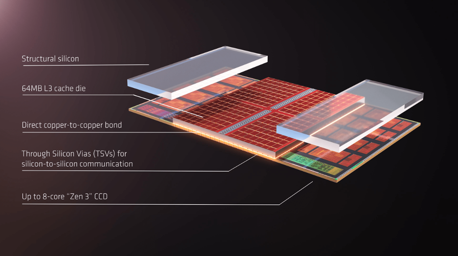
3D Stacking
3D stacking takes the concept further by stacking silicon vertically:
- Transistors and components are stacked on top of each other, creating a three-dimensional structure
- Vertical connections called Through-Silicon Vias (TSVs) connect the layers
- Benefits:
- Dramatically increased density in the same footprint
- Shorter distances between components, reducing latency
- Potential for much higher bandwidth between CPU and memory
- More efficient power delivery
Modern implementations include:
- Cache stacked directly on top of CPU cores
- Memory stacked on or very close to the processor
- Multiple compute layers stacked together
Alternative Computing Paradigms
- Quantum computing for specific types of problems
- Neuromorphic computing that mimics brain structures
- Optical computing using light instead of electricity
Next Steps
Now that you understand CPU basics, you might want to explore:
- RAM Basics: How computer memory works with the CPU
- How Semiconductors are Made: The fascinating process of creating CPU chips
- Computer Hardware Overview: The broader context of computer components
- Storage Technologies: How data is stored permanently